Tweets
proud to state that i did not pay for any of jeff’s ten-minute joyride to space. https://twitter.com/joroulette/status/1417512882271555587
(original)
https://twitter.com/josecastillo/status/1383807973617672195

(original)
Replying to @jasoncoon_, @adafruit, @seeedstudio, @oakdevtech and @GeekMomProjects
(original)
Replying to @fpgahelper
Thank you for these notes! This comment in particular suggests something I can look into tomorrow: I rather thoughtlessly changed some resistor values on this build to increase LED brightness. With the poor grounding job on this rev, it could be enough to cause issues.
(original)
Replying to @bikerglen
I’ve checked the clock source for the USB peripheral, at least: basically picking a pin and outputting a 500Hz PWM clocked from the DFLL. That seems to be working as expected; looks the same both on working and non-working boards.
(original)
Replying to @josecastillo
I have five of these panels; tomorrow I think I’m going to pull all of the parts off of one of the failed boards, and reassemble it on another panel but in the position of a board that succeeded.
(original)
Replying to @josecastillo
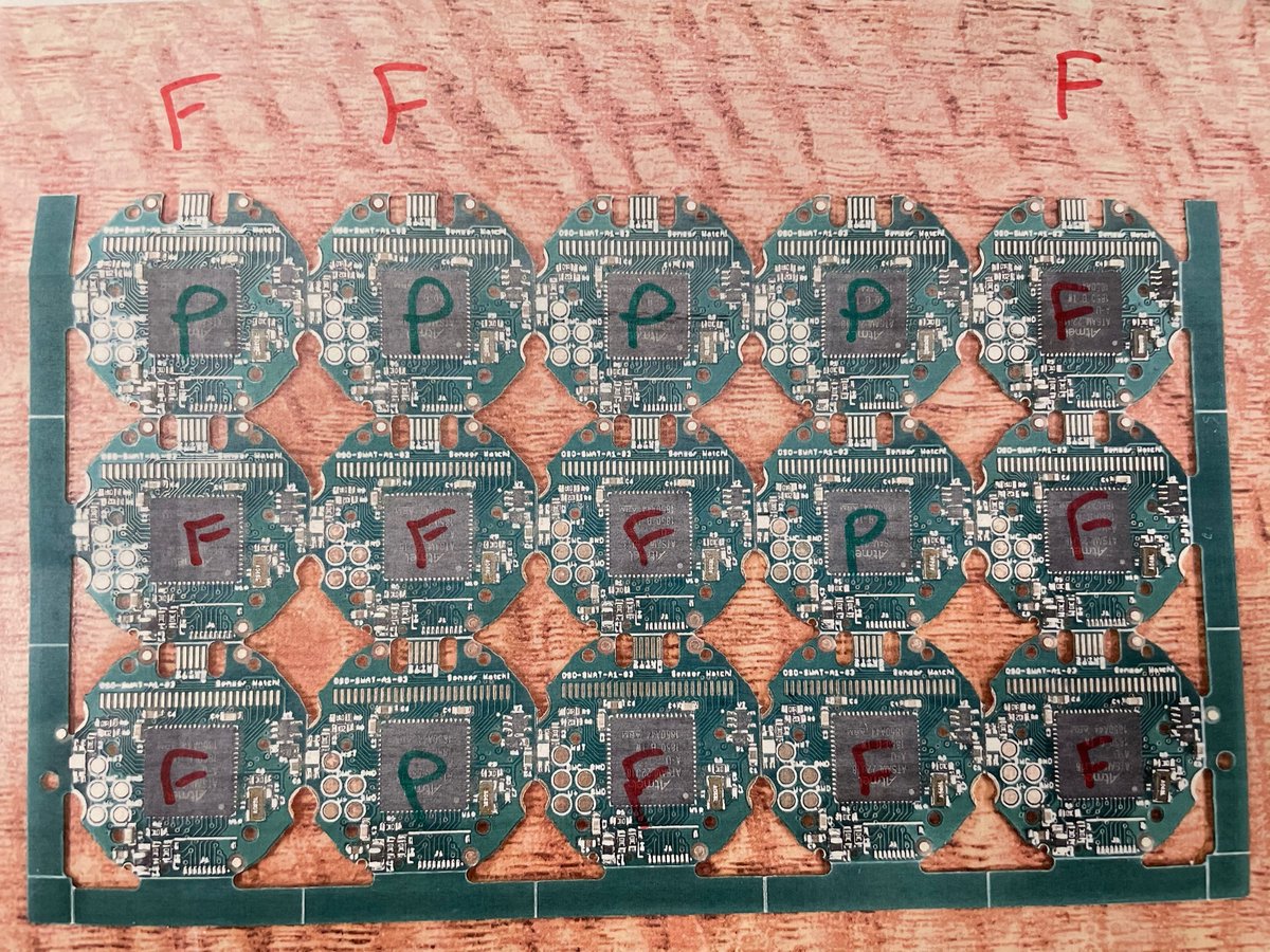
one other accomplishment for today though: tested all the remaining boards, and found that six of the 17 I assembled have working USB. So it wasn’t half a success, or half a failure. It was 65% failure. 😬
(original)
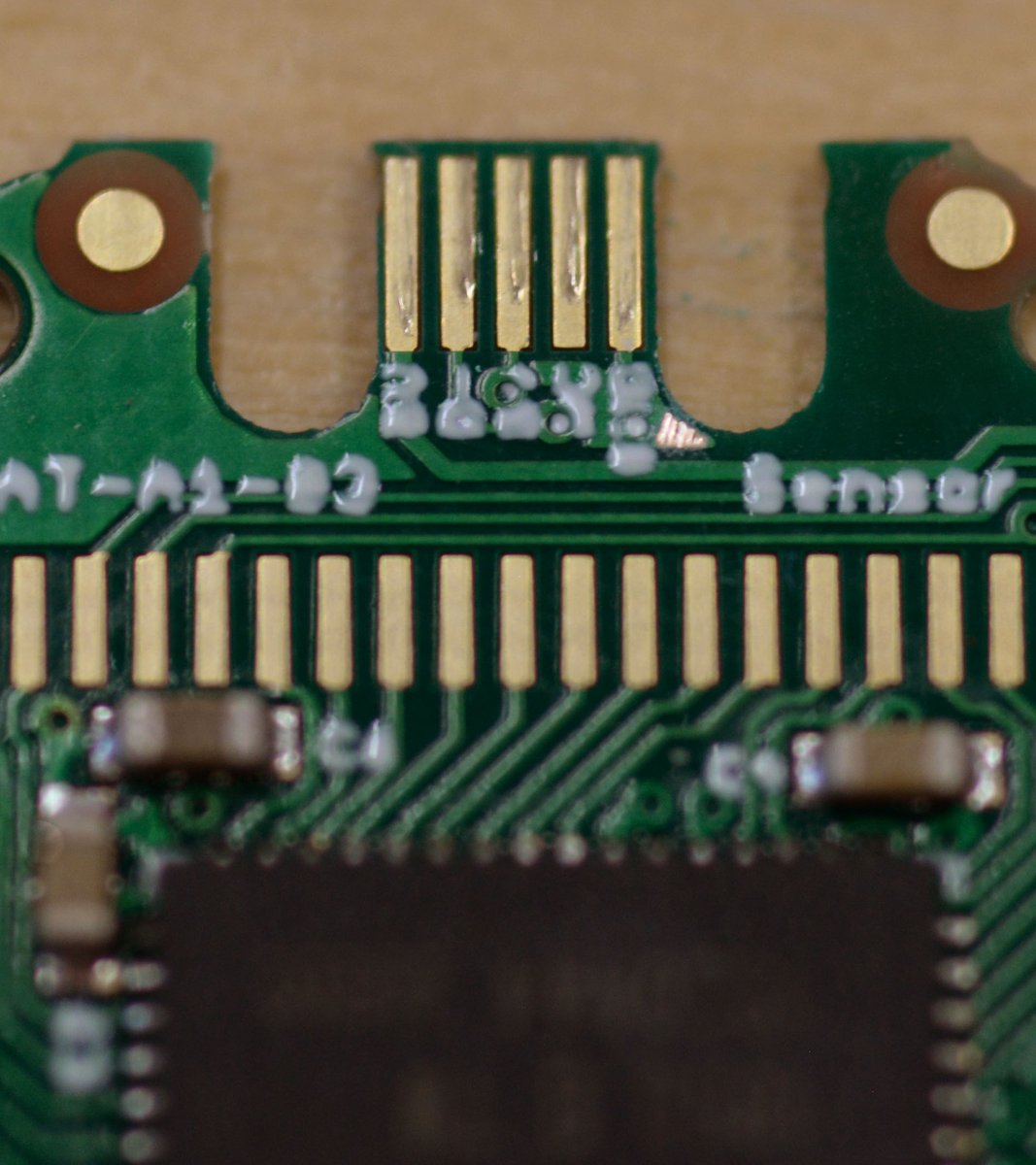
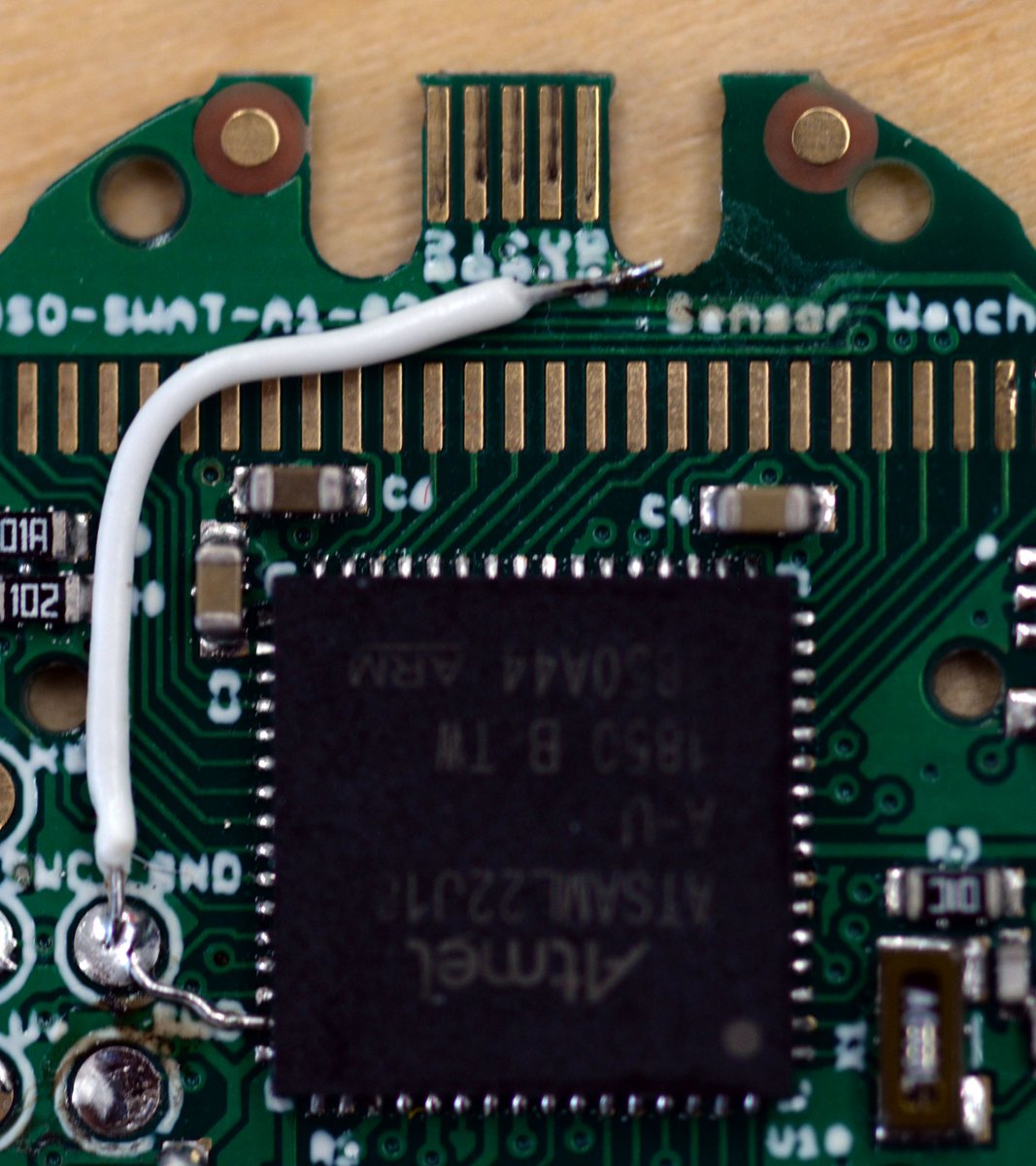
Well hmm. I bodged from the ground pour near the USB port (the triangle exposed with an X-Acto blade) to the GND pin near the USB pads, and… no change. USB still doesn’t function. so now I am doubly or triply confused. Maybe my bodge job sucked? either way the mystery continues.
(original)
Replying to @GregDavill
I tested the rest of the boards I assembled and ended up with six that seem to work fine, and 11 that won’t enumerate… going to put them all on the scope today and at least see if they all seem to fail in similar ways. but tbh I am not sure what I am looking at (yet)
(original)
Replying to @GregDavill
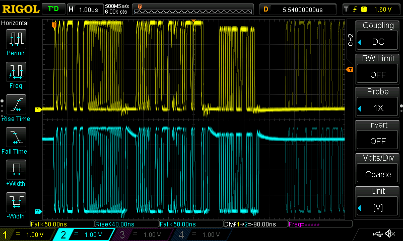
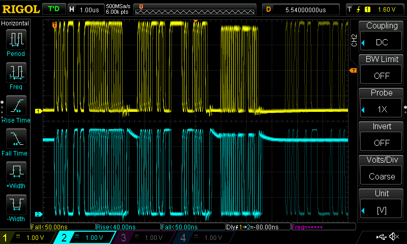
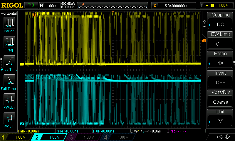
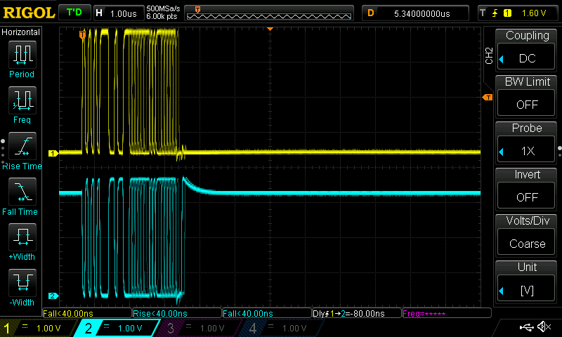
sure! The first one is what a working board looks like; #2 is a non-working board, which looks similar at first, but then the non-working board starts to do glitchy stuff like in #3. after that it looks like #4 and the signal seems to reset every couple seconds like in the video.
(original)
Replying to @SourceParts
I am optimizing for cost, also JLC only supports two layers at 0.6mm. the other thing is that I expect folks to use USB only rarely, to flash code onto the watch; then it goes in a watch case. I want it to work well, but it’s not like I expect folks to use the USB port every day.
(original)
Replying to @josecastillo
one interesting thing I’m noticing is that the output is cumulative, so you can prime it with a style (here, ‘glided’) and even once you set it to your new style (steampunk) it retains some elements of the first idea. (bonus throwback: ‘Cuil’ graffiti on the wall in that 1st one)


(original)
playing with the cloud supercomputer again; this time I fed the Cormac line to VQGAN+CLIP. I like that this one has a “style” parameter that I can use to tune the output; here’s the machine’s vision of the evil machine in steampunk, then with a dash of cyberpunk added at the end. https://twitter.com/josecastillo/status/1397434471557832704


(original)
Replying to @SilverCoaster
definitely and that is a planned activity for this week. Gonna be a challenge to solder to that QFN pad but I’ve done it before.
(original)
Replying to @impraxical
I could if I used a different board house like PCBWay (JLC’s 0.6mm boards are two layer only), but I’ve done USB on two layer boards in the past and had it work fine. Gonna keep fingers crossed and see if this change increases reliability; would like to try to keep it simple.
(original)
Replying to @mishkathebear and @timonsku
I will do that! thanks so much to both of y’all for your advice and suggestions on this!! 🙌🏽
(original)
Replying to @josecastillo
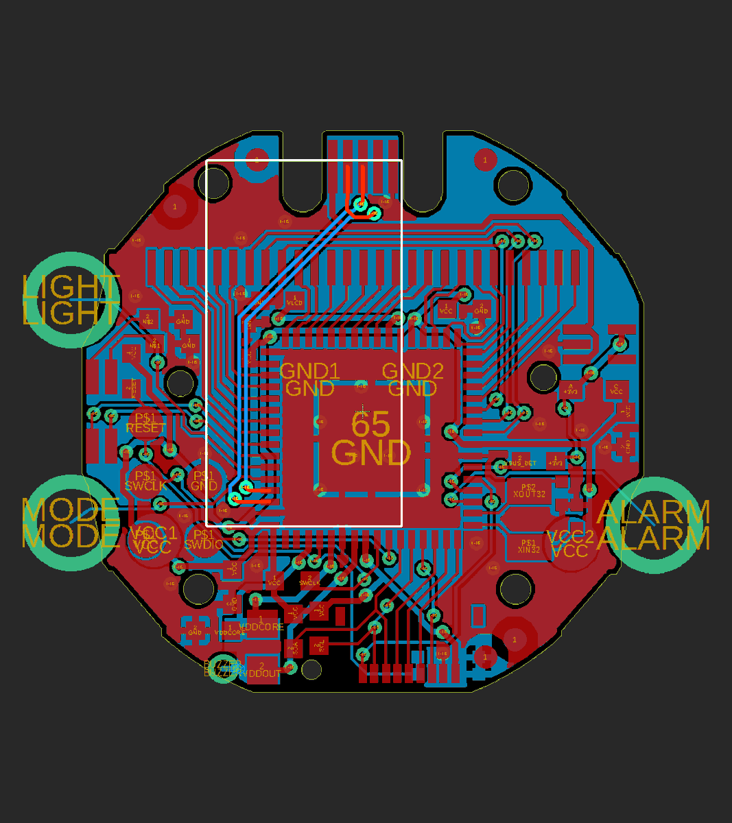
stitching might not be the right word here. “contiguousness”? anyway I can now feel confident that there’s a ground return path running right next to both the D+ and D- signals, meaning that in both cases the return path should be about the same length as the signal itself.
(original)
Replying to @josecastillo
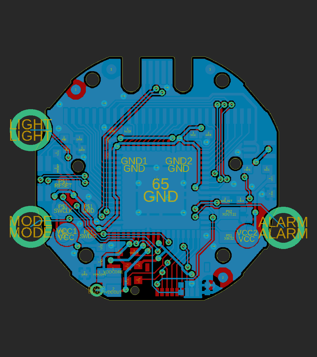
EPILOGUE: @timonsku makes the valid point that without a reference plane, there’s no reason to try to impedance match, and that it’s not even really worth it for 12Mbits USB. Figure I may as well make the traces thin and improve the ground plane stitching. This feels much better.
(original)
Replying to @timonsku
I actually considered it! But it has to be 0.6 mm thin to fit in the watch case, and JLC only has a two-layer service at that thickness.
(original)
Replying to @timonsku
Right, that makes sense… without a reference plane underneath, there’s really nothing useful an impedance calculator can tell me. I do think the GND return issue is the cause of my woes; none of my tests suggested mechanical issues, so fingers crossed the next revision nails it!
(original)
Replying to @josecastillo
but then there’s the other piece, and the sad ending to this thread: I am going to need to fabricate new boards and assemble them in order to test this fix. which means that this thing is unfortunately not as close as i thought it was. /thread
(original)
Replying to @josecastillo
As for the 17 boards I made this week, the USB seems to work on some of them! And the others work otherwise; you just have to program them with pogo pins and SWD. both of these classes of board seem useful for beta testing. working on a plan to get them out there to folks. 8/
(original)
Replying to @josecastillo
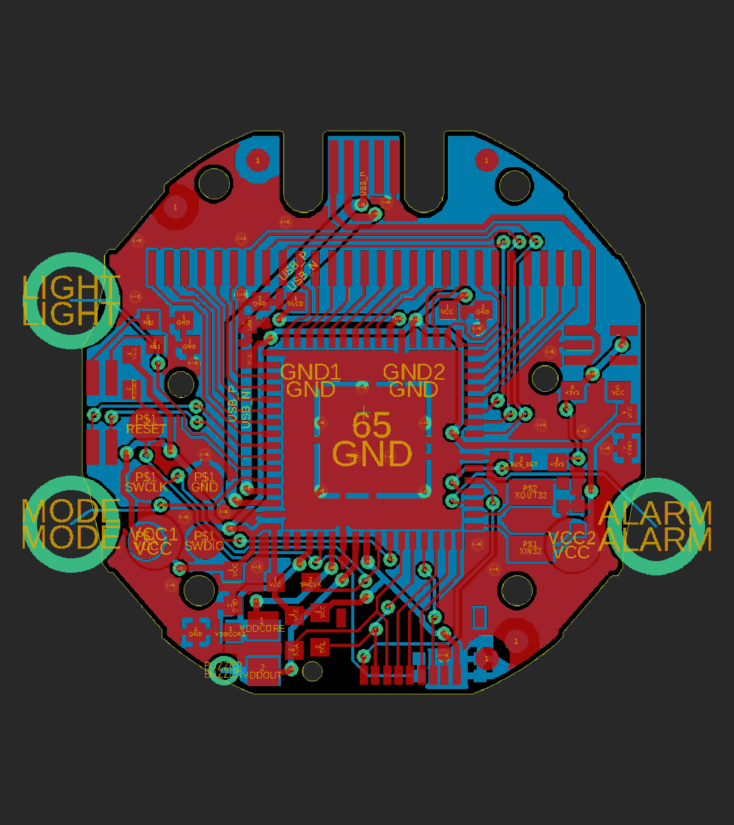
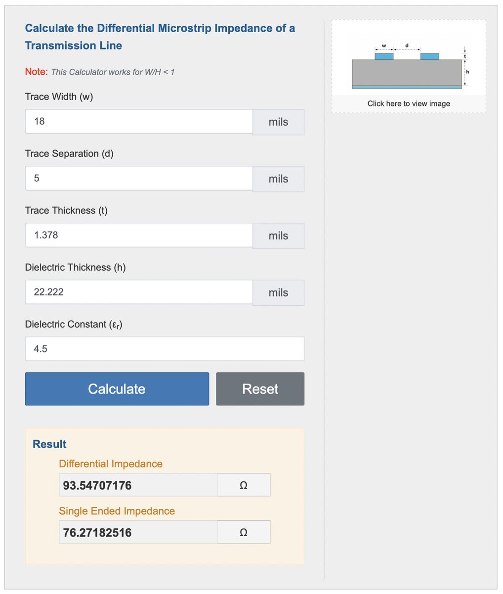
ANYWAY. The fix, I think. Just in case, I made the USB traces wider and routed them like a 90Ω differential microstrip. But more importantly: I rearranged the bottom ground plane to be one continuous, uninterrupted copper pour, and added a via by the MCU’s bottom left ground pin.

(original)
Replying to @josecastillo
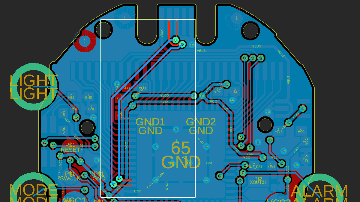
There’s also the issue that I made my USB traces really thin, and while I did length match them, I didn’t think about controlled impedance. consensus is that this may be less of a factor given the short trace lengths involved, but it’s another potential source of fail. 6/
(original)
Replying to @josecastillo
For a fast(ish) signal like full-speed USB, this can wreak havoc on signal integrity. And I think that’s what’s happening when I’m seeing the USB signals on the scope: the signal is unstable, and if it’s unstable enough, my computer gives up or tries to reset it to try again. 5/
(original)
Replying to @josecastillo
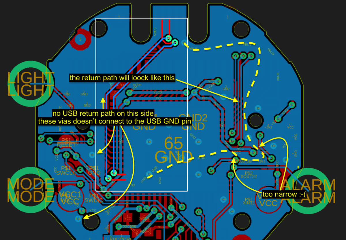
I added vias and scooted wires until all the ground plane islands were connected to each other, and the board passed DRC. but! looking closely it seems they’re connected via a maze of narrow copper bits, which makes for a meandering return path. (annotations by @mishkathebear) 4/
(original)
Replying to @josecastillo
So: for current to flow in a circuit, it has to flow from someplace and to someplace. In the case of this USB signal, it needs to flow back to ground. I used a ground pour on both sides to try to accomplish that. Unfortunately with only two layers, they’re not very contiguous. 3/
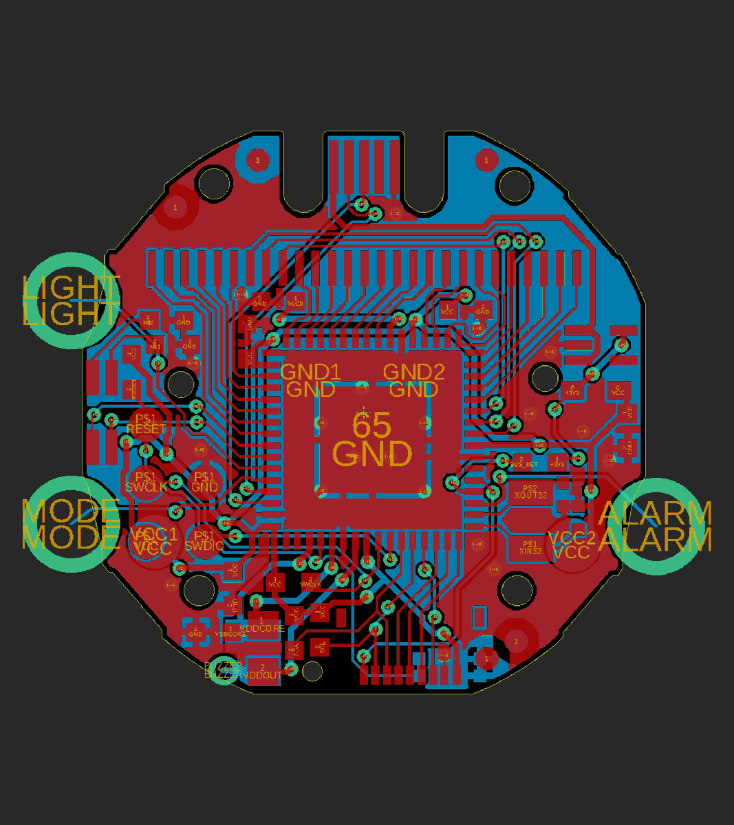
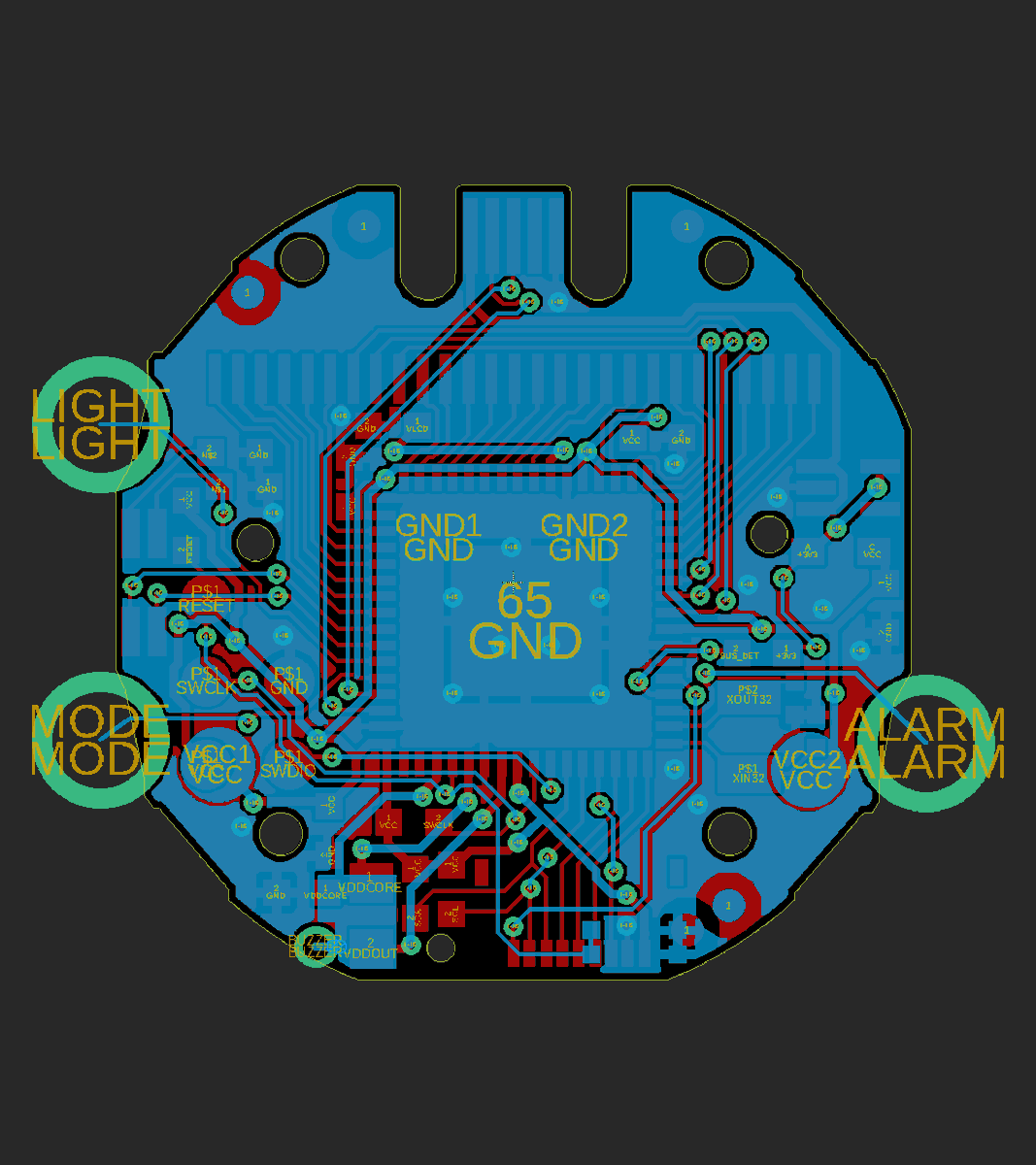
(original)
Replying to @josecastillo
(also if I get anything wrong here, feel free to correct me. this is a situation where I know I’m at the edge of my understanding; the only reason I have the insights I have here is thanks to help from folks like @mishkathebear @timonsku, @mattk and others who shared insights) 2/
(original)
At last, I think I have an answer for what’s gone wrong with USB on the watch. TL;DR: the theory is that I played fast and loose with my ground planes, and the USB signal doesn’t have a good return path to ground. This one is a bit esoteric. but worth unpacking in a thread. 1/9
(original)
Replying to @davedarko
Also might be worth looking into the @MicrochipMakes SAM L22. It has a built-in segment LCD controller, and the smallest G variant (48 pins in QFN and TQFP) has 23 segment LCD pins — just enough to drive that display. https://www.microchip.com/wwwproducts/en/ATSAML22G18A
(original)
Replying to @mishkathebear and @mattk
This makes a lot of sense… like it passes DRC because the islands are technically connected, but the return path for this signal meanders. There is a GND pin on the north (connected to the pad)… but even then, it really has to run the gauntlet to get there. Thank you for this!!
(original)
Replying to @mishkathebear and @mattk
Sure! tho that screenshot was my planned rerouting with wider traces. This is the board that I had fabricated and that I’m working with now, with the USB differential pair highlighted.
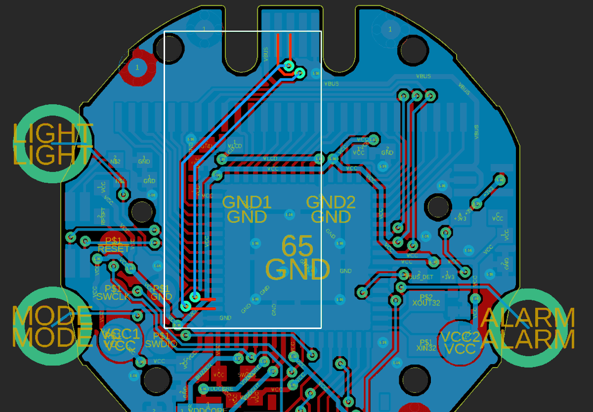
(original)
Replying to @timonsku, @mattk and @FauthNiklas
that’s definitely the other thing I want to test; my fear is that milling tolerances may be causing misalignment, i.e. what if on some boards the VBUS pin is overlapping with one of the signal pins when plugged in? but I haven’t had the time to chop up a USB cable and test it yet
(original)
Replying to @mattk
well hm. without upgrading to a 4 layer board I don’t think I’m going to get that adjacent ground plane. but then I’m not trying anything super speedy, and I’d hope that this could at least get me closer to a value that’s within tolerance? thanks for your guidance and suggestions
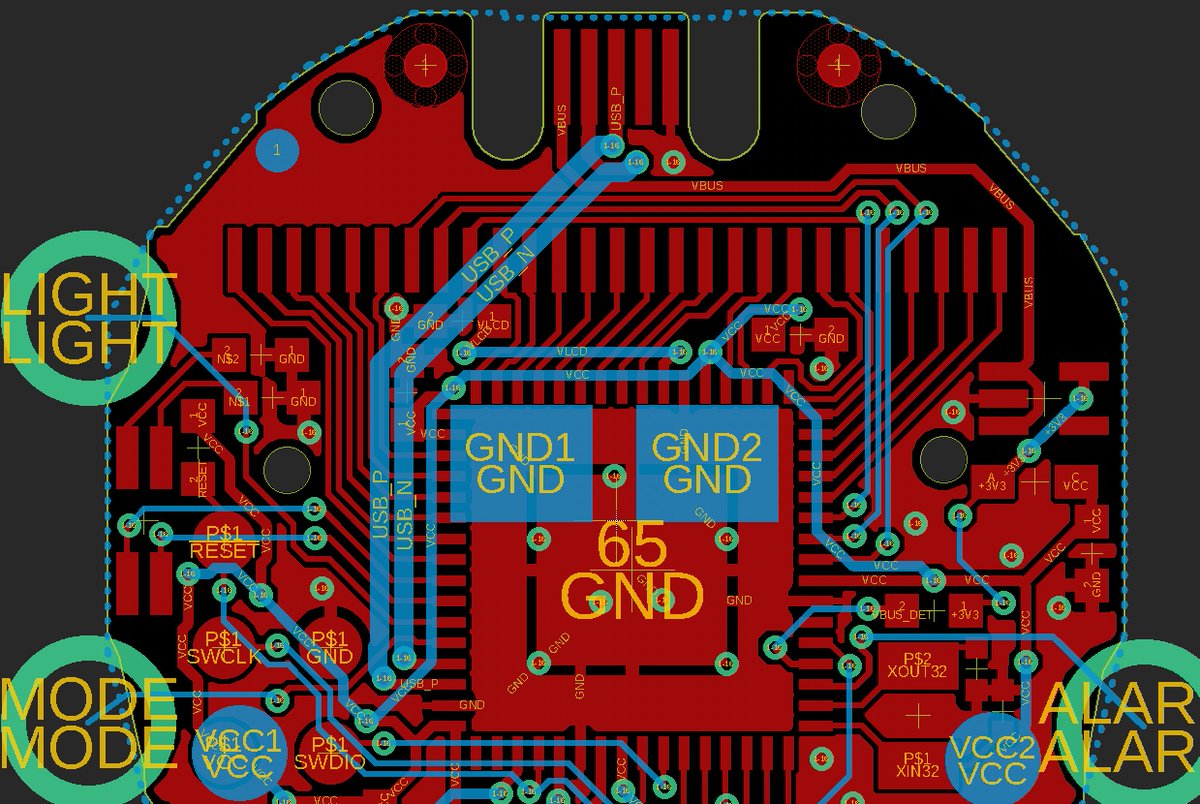
(original)
Replying to @mattk and @adafruit
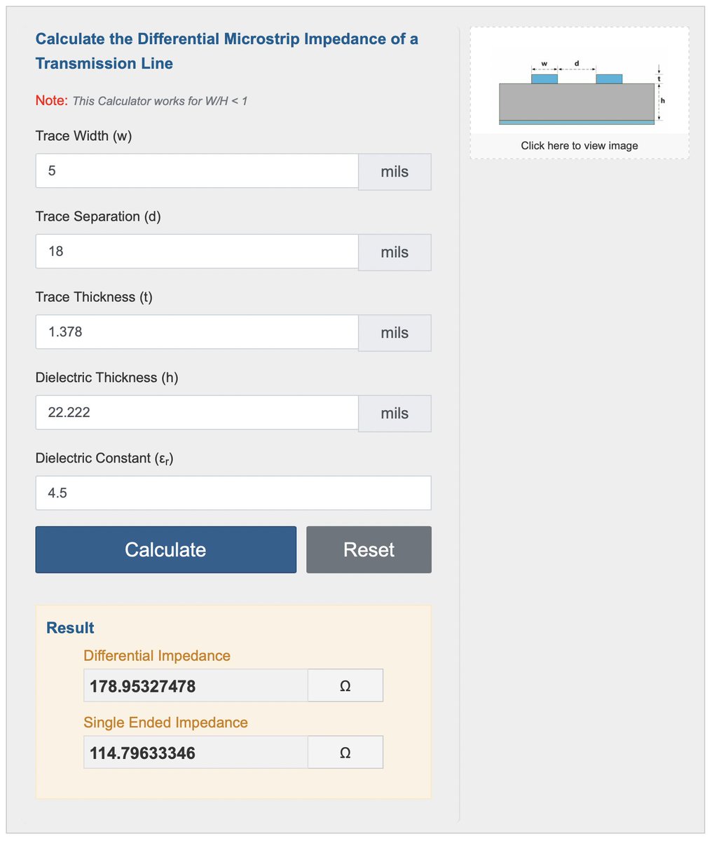
this may be the answer. I shrank most of my traces to 5 mil to get this board to route, but plugging in numbers for what I did, I get a differential impedance of 179Ω. which is wildly out of spec. I can reroute the USB with 18 mil traces, but you think this diagnosis makes sense?
(original)
A highlight from last night’s build: programming the watch boards with an @adafruit PyRuler. Using the Trinket M0 Arduino core and Adafruit_DAP to quickly flash the bootloader and set fuses. (bonus footage at the end: me being very confused about my USB enumeration glitch)
(original)
Replying to @josecastillo
question: did I have many dreams last night about being unable to solve this problem in front of a bunch of people? Answer: yes.
(original)
after sleeping on yesterday’s partial success (read: partial failure) with the boards, i have two theories of what might be going on. they’re both unpleasant. one more so than the other. full day for _dayjob today but hopefully I can test them out this evening.
(original)
Replying to @josecastillo
Thanks so much to everyone who joined and watched and shared questions and comments, including @bwshockley, @ElectronVillage and @sneenyc in the Periscope chat! Really appreciated the words of encouragement during a late night at the shop :)
(original)
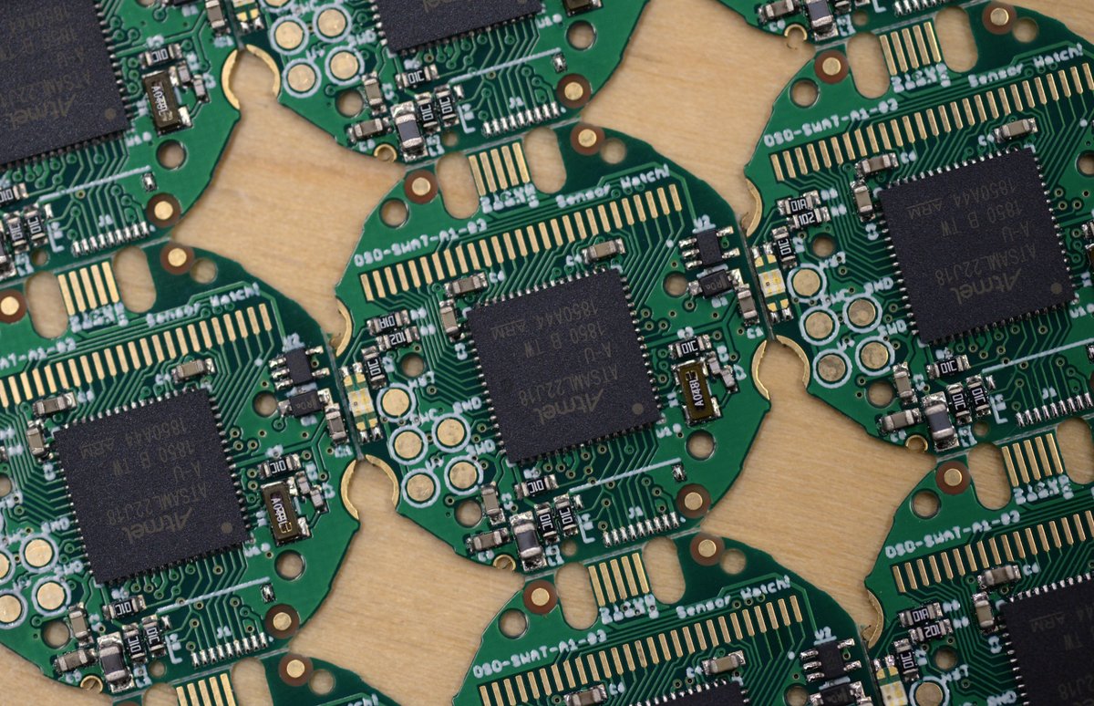
WELL THAT WAS FUN! I’m calling it a partial success. Good news: all of the boards seem to have fabricated correctly! Bad news: of the 7 I flashed with a bootloader, 3 exhibit the glitchiness. Which is an odd problem! But it’s also 10:00 PM, which makes it a tomorrow problem. 😬 https://twitter.com/josecastillo/status/1414735589555925015
(original)
RT @sneenyc: @josecastillo @the_prepared https://www.ti.com/lit/an/slva689/slva689.pdf?ts=1626073046128&ref_url=https%253A%252F%252Fwww.google.com%252F
TMI, if you’re into calculating exact I2C pullups
(original)
Replying to @josecastillo
I think I know what I’m doing now: you can reply here with questions or comments, OR you can comment in the Periscope chat and I should be able to see it and respond. OK, let’s get to it!
(original)
Live from the workshop of @the_prepared in Brooklyn, New York: let’s do this thing! Building a panel of Sensor Watch PCB’s. https://www.pscp.tv/w/c7t8zzFyYWpaeU5Eb0FuS3p8MXlwSmRnRW5EQm9HV4AhqESKsVgQ9XbsPnBaI4R07NJQuZwwUtXEvGCKppT2
(original)
if I can get my shit together, I should be live-streaming the assembly of this first panel of watch PCB’s in just under half an hour (7:45 EDT / 4:45 PDT); link will be in the feed. Will I face the bootloader glitch? IDK, but sometimes you gotta just do the thing. #YOLO
(original)
Replying to @sneenyc
i think the thrill of it is that it *might* write a blink sketch, but if it writes an impossibly large buffer overflow instead, you can’t say you weren’t warned…
(original)
speaking of technology that I’m convinced has to be a prank: GitHub Copilot? Like, as an April Fool’s joke, an AI that writes SQL injection vulnerabilities into your code is pretty funny. But releasing it as actual product is really committing to the bit. https://gist.github.com/0xabad1dea/be18e11beb2e12433d93475d72016902
(original)
Replying to @josecastillo
well hmm. fixed one board just by re-reflowing it. some of the previous gen boards don’t seem as receptive to this fix. but it at least proves that the current revision can/should work. anyway. too late to build boards today. but maybe I’ll stick around late at the shop tomorrow.
(original)
Update: not assembling watch boards today. The bootloader isn’t working as well as it should; double tap enters the right mode, but some boards fail to enumerate over USB (and act generally cursed when plugged in). i need to figure out what’s going on before I can move forward.
(original)
Replying to @songsteven2
not this user.
(original)
Replying to @derekcaelin
I think it has clarity and simplicity, affordances like window borders and lightweight skeuomorphism that makes it accessible. But mostly I like that it respects the user enough to let them customize the UI. It feels empowering to tell people “this is your computer; have at it.”
(original)